
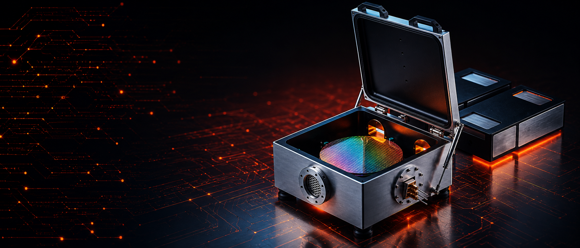
MWA Front-End (FEOL) Applications:
Source/Drain Dopant Activation - Ultra-shallow junction formation for advanced logic nodes
Extension Implant Activation – Precise activation with minimal dopant diffusion
Implant Damage Recovery – Crystal lattice repair following ion implantation
FinFET Device Processing – Low thermal budget annealing for FinFET structures
Gate-All-Around (GAA) Processing – Activation and defect repair for nanosheet devices
Silicide Formation – Low-resistance contact formation for source, drain, and gate regions
Contact Resistance Reduction – Improved electrical performance at critical interfaces
Interconnect Annealing – Metal and dielectric optimization while protecting low-k materials
Compound Semiconductor Processing – GaN, r-GeO2, GeSn and SiC device thermal treatments
Emerging Memory Devices – MRAM, ReRAM, and other next-generation memory applications
MWA Back-End (BEOL) Advanced Packaging Applications:
Hybrid Bonding Anneal – Improved Cu-Cu and dielectric bond quality
Wafer-to-Wafer Bonding – Enhanced interface strength for 3D integration
Die-to-Wafer Bonding – Low-temperature post-bond annealing for heterogeneous integration
Chiplet Integration – Thermal processing compatible with advanced chiplet architectures
2.5D Interposer Assembly – Reduced thermal stress during package integration
3D IC Stack Processing – Annealing for vertically integrated semiconductor stacks
TSV (Through-Silicon Via) Processing – Stress relief and electrical performance optimization
Fan-Out Wafer-Level Packaging (FOWLP) – Low-temperature processing of redistribution layers
System-in-Package (SiP) Assembly – Thermal treatment for multi-die package integration
Heterogeneous Integration – Processing of mixed materials and device technologies with minimal thermal impact